SK materials performance
About the Company
SK materials performance is a polymer materials research company that develops and produces photo materials essential for drawing semiconductor circuits. Based on innovative R&D capabilities, SK materials performance is expanding beyond semiconductors to light-responsive displays and image sensor materials, advancing the cutting-edge future.
Based on advanced R&D capabilities, SK materials performance develops and supplies materials such as Photo Resist, Bottom Layer Anti-Reflection Coating(BARC), and Hardmask(SOC_Spin on Carbon), which is required for the lithography process of drawing semiconductor circuits. across industries.
Future Growth
- Based on the binder technology acquired while developing materials such as PR, Barc, and SOC, which are essential for semiconductor manufacturing, SK materials performance is expanding the application field of technology from semiconductors to displays and batteries, etc.
- It is developing existing semiconductor materials into high value-added business by developing advanced products such as EUV PR following technology refinement, and expanding the portfolio limited to PR materials for pre-processing to Advanced Package materials(PR for plating, etc.) and display materials(Mini / Micro Lens).
- Based on SOC-based materials, it is preparing new markets such as high-refractive Encap and lenses for displays, and based on existing PR and SOC technologies, and intends to expand its portfolio to color filters, etc., which are high-value CIS materials in the high-tech sensor market.

Photo Resist
It is a material that forms an image pattern by causing a change in solubility in the developer when exposed to light and radiation energy, and it is a liquid material composed of polymers, photosensitizers, additives, and solvents.

Types of Photo Resist
- According to the wavelength of the light source, it is divided into I-line(about 365nm), KrF(248nm), ArF(193nm), and EUV(13.5nm), and the narrower the width of the wavelength, the more micro circuits can be drawn.
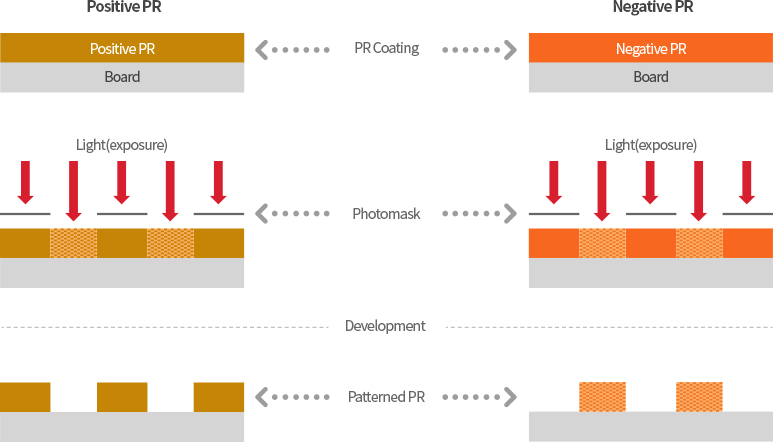
- It can be divided into Positive PR, in which the area exposed to light melts, and Negative PR, in which the area that is not exposed melts.
- SKMP is a material used in the photolithography process in the production of semiconductors for DRAM and NAND. We have various product lines from and ArF Imm PR to high-thickness bump PR for post-processing, and are developing EUV PR products according to advancement and refinement of semiconductor technology.
Photo Resist (PR) Types and Characteristics
Bottom Layer Anti-Reflection Coating(BARC)
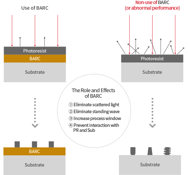
- It is a material that minimizes the loss to pattern profile by suppressing the scattering and reflection of light from the substrate generated during the exposure process.
- SKMP's BARC products have an excellent coating, ranging from ArF Imm BARC to KrF BARC, and a high refractive index(n) that allows to achieve physical properties with minimal thickness.
Hardmask(SOC)
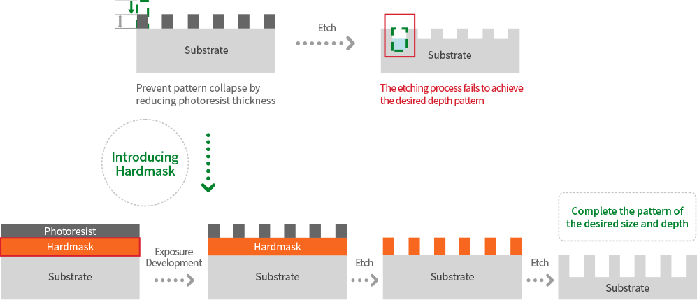
- As the thickness of the PR becomes thinner and the size of the pattern becomes smaller due to the high integration of the semiconductor, the collapse of the PR pattern occurs. Therefore, it is not possible to etch the layer using the PR pattern, so the hardmask (SOC), a representative material with strong etching resistance, is introduced between the PR and the layer to be etched.
- SKMP's SOC products with strong etching resistance and flattening characteristics range from 400 Å to 3 μm thickness, and we are developing excellent SOCs that meet the characteristics of process according to customers and the development of semiconductor technology.